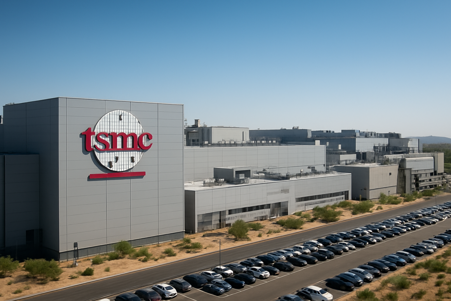
TSMC Reportedly Plans 12 Fabs and 4 Packaging Facilities in Arizona
New reports suggest TSMC is planning a massive expansion in Arizona, targeting 12 advanced fabs and four packaging facilities as part of a major investment strategy.
Key Points
- TSMC is reportedly planning to expand its Arizona presence to 12 advanced fabs.
- The expansion includes four advanced packaging facilities and an R&D center.
- The company acquired 900 additional acres, bringing its total campus to 2,000 acres.
- Total investment for such an expansion could exceed $100 billion.
- The plan aligns with a broader $500 billion U.S.-Taiwan investment agreement.
In a development that could reshape the global semiconductor landscape, recent reports from DigiTimes suggest that TSMC is planning a massive expansion of its U.S. operations. The company is reportedly considering an expansion of its Arizona site to include 12 advanced fabs, four packaging facilities, and at least one research and development center. This ambitious roadmap is purportedly part of a broader intergovernmental deal between the United States and Taiwan, aimed at injecting $500 billion into various American high-tech sectors. Rumors regarding TSMC's intentions to expand its presence near Phoenix, Arizona, have circulated for quite some time, though the company has remained cautious, stopping short of official confirmation. Back in early March, reports suggested a target of 10 advanced fabs. However, the latest intel suggests the company is looking to build an additional Gigafab complex adjacent to its existing Fab 21, pushing the total count to 12. While these numbers are significant, they should be viewed as industry speculation until formal project milestones are announced. The scale of this expansion is supported by recent real estate moves. TSMC recently acquired approximately 900 acres of land adjacent to its existing 1,100-acre campus, bringing the total footprint to 2,000 acres. To put this in perspective, the facility is now effectively the size of a small town. This acquisition, coupled with industry chatter regarding a potential $100 billion increase in investment, strongly suggests that the company is preparing for a major build-out of its Fab 21 site and potentially other regional locations. Building a leading-edge logic fab is an incredibly capital-intensive endeavor. A modern 2nm-class fab module, with a capacity of roughly 20,000 wafer starts per month, carries a price tag between $25 billion and $35 billion. Consequently, building six or more advanced fab modules—which will likely utilize 1.4nm or even more advanced lithography processes—will require an investment significantly higher than $100 billion. This underscores the sheer scale of the financial commitment required to sustain a competitive edge in the semiconductor industry. Despite the "where there's smoke, there's fire" nature of these reports, it is important to remember that plans in the high-tech industry are fluid. Even if TSMC has strategic reasons to expand, it appears that no final, binding plans have been signed off. Market fluctuations, supply chain availability, and regulatory environments play a massive role in these decisions. Therefore, while the reported expansion is a strong indicator of intent, the final implementation may differ from current rumors. Advanced packaging facilities are becoming just as critical as the fabrication process itself. As chiplet designs and 3D stacking become standard in high-performance computing, the ability to assemble these components domestically in the U.S. provides a strategic advantage for companies like Apple, NVIDIA, and AMD. By localizing both the manufacturing and the packaging, TSMC is effectively creating a self-sustaining ecosystem that reduces reliance on overseas logistics. Ultimately, the potential for 12 fabs in Arizona marks a significant shift in the global supply chain. This expansion is not merely about building factories; it is about securing the future of the American tech sector. As the demand for AI hardware, cloud computing, and consumer electronics continues to skyrocket, having a domestic manufacturing powerhouse will be vital for long-term growth. We will continue to monitor these developments as more concrete information becomes available.
Strategic Expansion in Arizona
TSMC aims to scale its production capacity by constructing a massive complex featuring 12 fabs. This expansion is designed to localize advanced manufacturing nodes (such as 2nm and 1.4nm) within the U.S., significantly enhancing global supply chain resilience. This strategy is backed by a substantial increase in property holdings, indicating a long-term vision that extends beyond mere production volume to the creation of a fully integrated industrial ecosystem.
Financial and Logistical Hurdles
Constructing these facilities requires massive capital expenditure, with individual module costs reaching tens of billions of dollars. Building 12 units represents a gargantuan financial undertaking that necessitates complex coordination and a highly skilled workforce. Advanced packaging remains a critical component of this roadmap, as it is essential for optimizing chip performance and efficiency, serving as a cornerstone for current and future semiconductor competitiveness.
This article was drafted with AI assistance and editorially reviewed before publication. Sources are listed below.